
제 25회 반도체 대전 SEDEX
October 25 ~ 27 / COEX SEOUL

2023 참가업체 디렉토리
(주)제브
GEV co., Ltd.
Booth No.- CEO하태성 / Ha Taeseong
- ADDRESS충청북도 음성군 맹동면 맹동산단로 37-10 / 37-10, Maengdongsandan-ro, Maengdong-myeon, Eumseong-gun, Chungcheongbuk-do, Republic of Korea
- CONTACTTel. +821049349204 / Fax. 82-043-715-7555 / URL. http://www.gevkorea.com
-
제조품목
전력 반도체 스위칭 특성 향상 솔류션 제공
▶▶ (주)제브는 귀사 제품(전력 반도체)에 대하여 전자빔 조사 공정 수탁 처리 합니다.
실리콘 웨이퍼, 다이오드 또는 IGBT의 스위칭 속도, 복구 시간 및 기타 전기적 특성을 높이면 경쟁 우위를 높이고 대상 산업에서 더 큰 시장 점유율을 얻을 수 있습니다.
방사선 기반 전자빔 (E-Beam) 처리는 IGBT, SCR, BJT 및 GTO와 같은 많은 양극성 실리콘 전력 반도체 장치의 스위칭 속도(전력 반도체에 대한 소수 캐리어 수명 제어)를 조정하기 위한 안정적이고 재현 가능한 방법입니다. 이(수명 제어를 위한 중금속 확산)는 금 또는 백금 도핑의 기존 공정에 비해 상당한 이점을 제공합니다.
-E-빔 조사 효과는 후속 어닐링을 통해 완전히 되돌릴 수 있습니다.-쉽게 제어되는 균일성 및 높은 재현성-웨이퍼뿐만 아니라 최종(패키지) 디바이스까지 처리할 수 있는 능력전자빔 조사는 안정적이고 재현 가능합니다.
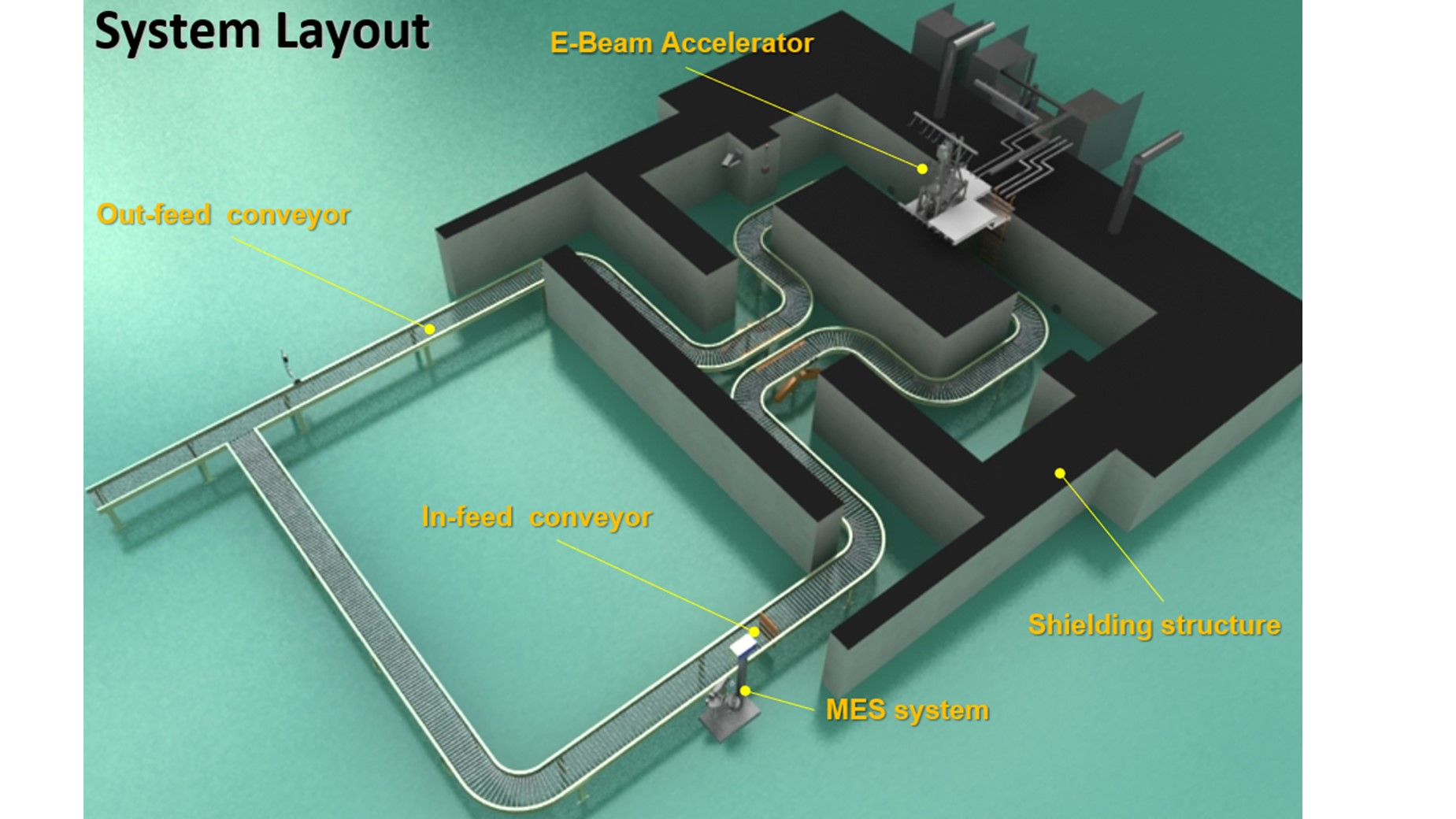
당사의 웨이퍼 캐리어는 비용 효율적인 처리를 위해 단일 실행으로 웨이퍼 스택을 처리할 수 있을 뿐만 아니라 스택 전체와 웨이퍼 전체에 걸쳐 균일한 선량 흡수를 허용합니다.
-아시아에서 최대 10MeV의 전자빔 에너지-전문적인 품질 보증 절차를 준수하여 매번 정확한 용량 적용-국내 및 해외 물류 경험을 통해 개발된 빠르고 안정적인 배송 시간E-Beam을 사용하여 수많은 반도체의 기능 향상 달성
·다이오드·사이리스터·게이트 턴오프 사이리스터(GTO)·절연 게이트 양극 트랜지스터(IGBT)·양극성 접합 트랜지스터(BJT)·전력 MOSFET(바디 다이오드)·실리콘 웨이퍼·태양 에너지 산업 내 구성 요소·전기자동차 산업 내 부품 프로젝트를 시작하려면 저희에게 연락하세요.PNG "%EC%BA%A1%EC%B2%98(1).PNG")
Material Modification Solutions for Power Semiconductors
By increasing the switching speed, recovery times, and other electrical properties of your silicon wafers, diodes, or IGBTs, you can increase your competitive advantage and gain greater market share in the industries you target.
Radiation-based Electron Beam (E-Beam) processing is a reliable and reproducible method for tailoring switching speeds (minority carrier lifetime control for power semiconductors) of many bipolar silicon power semiconductor devices such as IGBTs, SCRs, BJTs, and GTOs. This (heavy metal diffusion for lifetime control) offers significant advantages over the conventional processes of gold or platinum doping:
-The E-Beam irradiation effect is fully reversible through subsequent annealing-Easily controlled uniformity and high reproducibility-The ability to process not only wafers, but also final (packaged) devicesE-Beam irradiation is reliable and reproducible
Our wafer carrier not only allows for the processing of stacks of wafers in a single run for cost-effective processing, but also allows uniform dose absorption throughout the stacks and across the wafers.
-E-Beam energies up to 10 MeV in South Korea and Asia-Correct dose application every time, by adhering to professional quality assurance procedures-Rapid and reliable turn times developed through experience in domestic and international logisticsUse E-Beam to achieve feature enhancements in numerous semiconductors
·Diodes·Thyristors·Gate Turn Off Thyristors (GTOs)·Insulated Gate Bipolar Transistors (IGBTs)·Bipolar Junction Transistors (BJTs)·Power MOSFETs (their body diodes)·Silicon wafers·Components within the solar energy industry·Components within the electric vehicle industry Contact Us To Get Your Project Started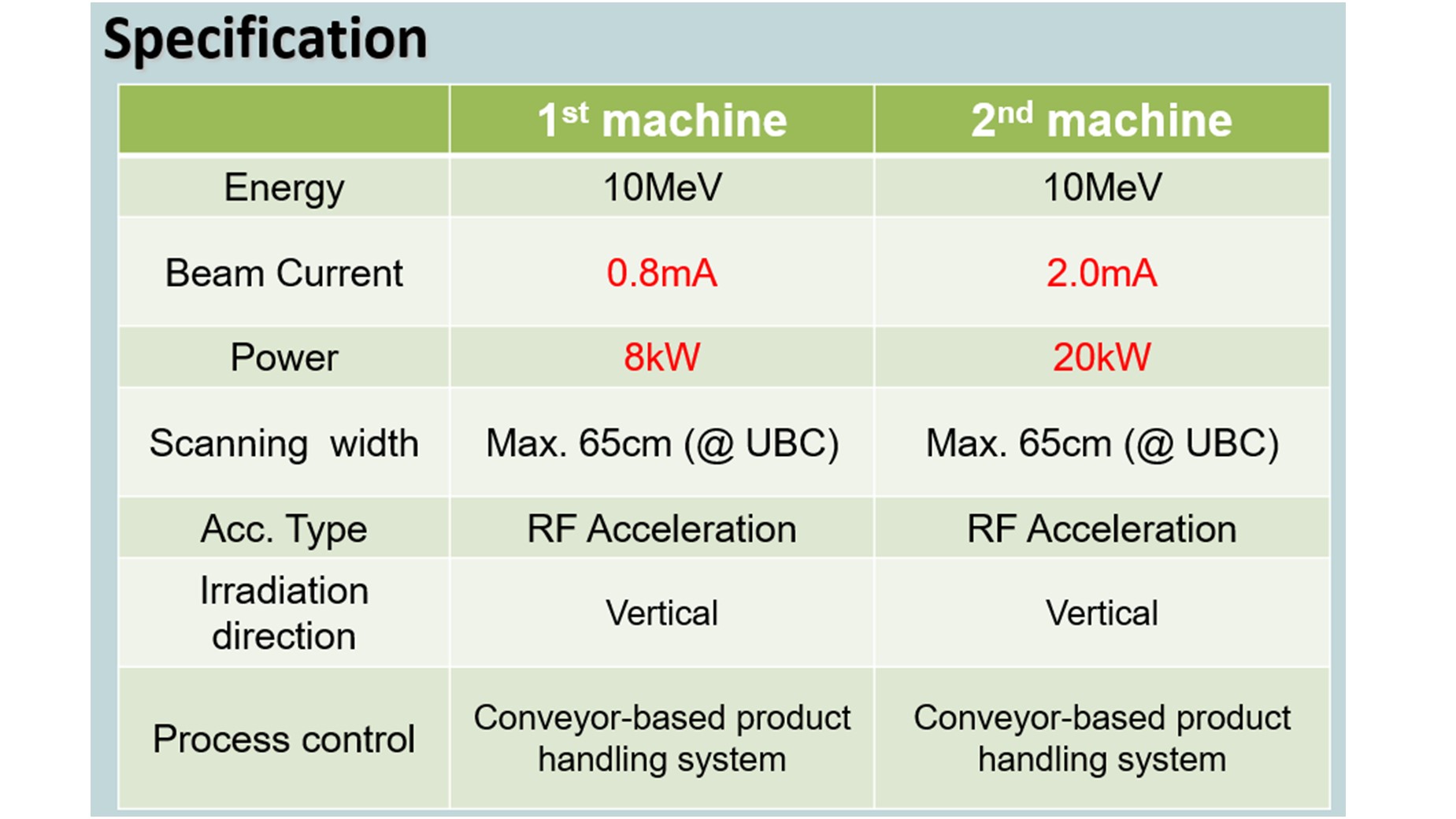

-
회사소개
(주)제브는 귀사의 전력 반도체에 대하여 전자빔 조사 공정을 제공합니다.
(주)제브는 어떻게 귀사에게 도움이 될 수 있습니까?
▶안전하고 효과적인 처리를 보장하는 맞춤형 솔루션▶제조 또는 유통 허브 근처에 위치한 글로벌 통합 시설 네트워크▶안전 표준을 뛰어 넘는 고품질의 일관된 프로세스▶신속한 제품 처리 서비스자세한 내용은 전화로 문의하세요.
043-882-7337
Benefits of E-Beam Services by GEV
▶Uniformity control▶High reproducibility▶ISO 9001 certificationHow can GEV’ expertise help you?
·Customized solutions to ensure secure, safe, and effective processing·A global integrated network of facilities located near your manufacturing or distribution hubs·High-quality and consistent processes that exceed safety standards·Expedited product processing servicesCall Us for More Information
South Korea +82-43-882-7337 -
소개영상
-
온라인 상담스케쥴
반도체대전에 대한 안내 날짜/시간 10:00 11:00 12:00 13:00 14:00 15:00 16:00 10월 25일 10월 26일 10월 27일
- Tel : +82-2-570-5229
- Fax : +82-2-570-5269
- E-mail : sedex@ksia.or.kr